After abandoning the bridge-IC approach, I went looking for something that didn’t require me to maintain a desktop application. The Bus Pirate had been in the back of my head for the whole project — that’s a microcontroller with a serial console glued to a level-shifted IO bank, and it just works wherever there’s a terminal emulator. That’s the model I should have started with.
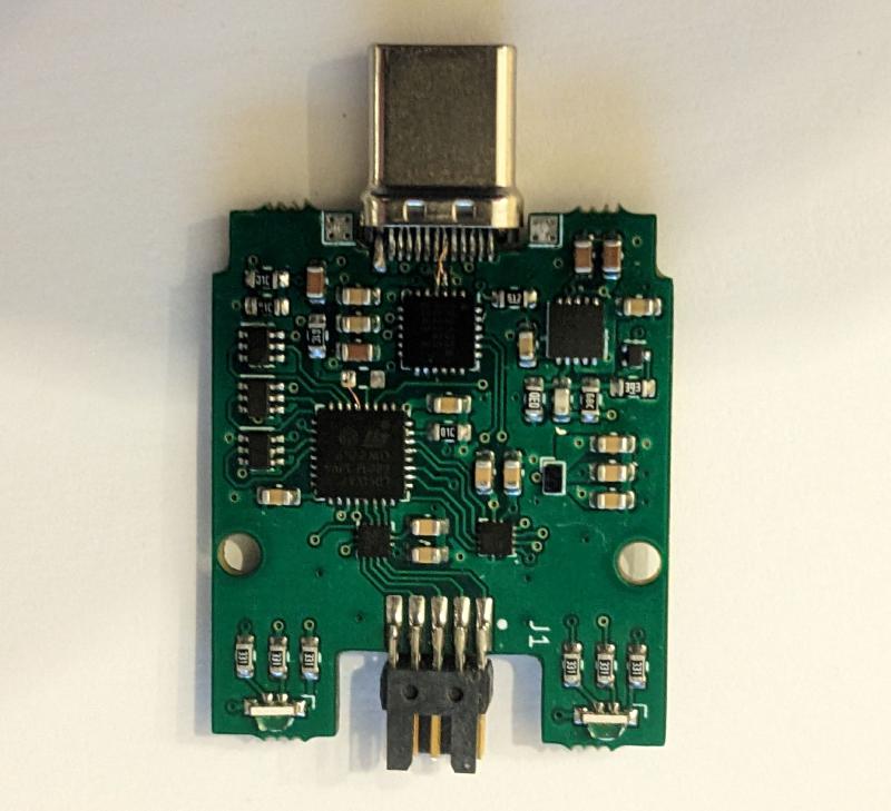
So Version 2 is an STM32, a USB-to-UART bridge, level shifters, and the power topology from V1. The user interface runs as firmware on the MCU, accessible over a serial console on the host.
Why an MCU buys more than I expected#
The obvious win is that the console is part of the device. Any OS with a serial terminal can talk to it. No drivers to write, no installers, no signed binaries.
The less obvious win is that the MCU has spare peripherals I didn’t ask for and now want to use. Input capture timers turn into a frequency counter on an idle pin. A free GPIO becomes a logic-level monitor. ADCs become a crude voltmeter. The CY7C65215 has GPIOs too, but no programmable peripherals you can repurpose — no input capture, no ADC, no DAC. The bridge-IC approach put a ceiling on the feature set; the MCU approach puts a floor on it.
Host link and reprogramming#
The host side runs through a CP2102N USB-to-UART bridge, not the STM32’s own USB peripheral. The honest reason is that I hadn’t worked with USB CDC firmware before and I had worked with UART bridges plenty of times. Going with what I knew got the board done faster, at the cost of a part I could have eliminated. If I were starting over today with the time to learn it, dropping the bridge and using the STM32’s USB peripheral directly would be the cleaner design — one fewer chip, one fewer footprint, and the bootloader path would still work because STM32s also have a USB DFU bootloader in addition to the UART one.
That same UART path handles reprogramming for now. The STM32’s built-in UART bootloader means the cable I use to talk to the device at runtime is the cable I use to reflash it. No ST-Link, no soldered jumpers, no taking the case off. That was worth designing around — firmware updates are going to happen on a project like this, and not having to dismantle the module for each one mattered.
Level shifting#
The MCU doesn’t have a configurable VCCIO pin like the CY7C65215 did. Whatever rail it runs on is what its pins swing to. To get 1.8 / 3.3 / 5 V on the bus side, I need a level shifter between the MCU and the connector.
I could have rolled my own — MOSFET, two resistors, the usual circuit per line. Space is tight enough that I went with an integrated shifter chip instead. Less area, less to debug, fewer parts to place by hand.
The constraint that drove the rest of the design is that integrated shifters have a fixed A-side and B-side, and the part requires VccA ≤ VccB. To keep that relationship valid across all three bus voltages, the MCU side has to sit at or below the lowest of them. Otherwise a 5 V bus needs the MCU on the low side and a 1.8 V bus needs the MCU on the high side — different orientations, which a fixed-pin shifter can’t do.
Putting the MCU at 1.8 V resolves that. The bus side is always equal or higher, one shifter handles all three levels, and the cost is a selection criterion for the MCU: it has to run at 1.8 V. That ruled out a chunk of the STM32 catalog but left plenty to choose from.
Power#
Three rails now, instead of two:
- 5 V from USB VBUS, used both as the bus-side 5 V case and as input to the regulators.
- 1.8 V fixed, for the MCU.
- 1.8 / 3.3 V adjustable, for the bus-side IO via the level shifters.
The adjustable rail still uses the feedback-network-with-a-MOSFET trick from V1. That part of the design was fine and I kept it.
Rather than drop a second standalone LDO in for the fixed 1.8 V, I picked a dual-channel regulator with one channel fixed and the other adjustable. One package, one set of capacitors, fewer footprints on a 20 mm board. The 5 V handoff still goes through the FPF1320 power multiplexer, so the rail crossover is unchanged.
The rest of the board is the same idea as before, with the bridge chip replaced by the MCU and a level-shifter bank.
Where it’s at#
Hardware works. Firmware is the next problem, and it’s where this is going to live for a while — getting the console behavior right, deciding how protocol modes are selected and configured, what the help text looks like, all the small UX choices that turn a board into something usable. I’ll write that up separately when there’s a real thing to say.
The whole project is on GitLab if you want to look at the schematics, layouts, or BOM.