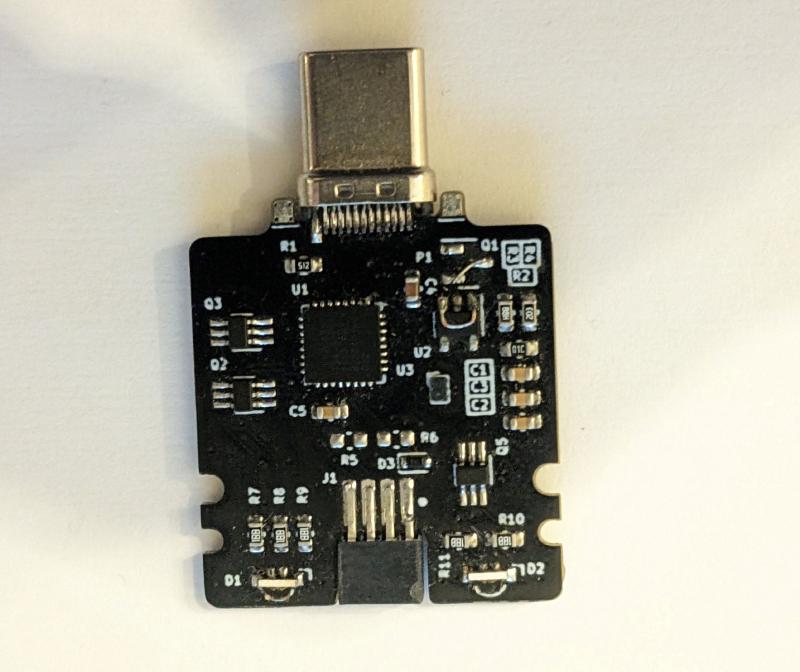
The first version was built around one idea: pick a USB-to-serial bridge chip that already speaks all the protocols I want, then wrap a power supply around it that can shift IO levels on the fly.
The chip I landed on was the Cypress (now Infineon) CY7C65215. It supports I2C, SPI, and UART, exposes a stack of GPIO, and has JTAG-capable variants in the family if I wanted to grow into it later. Crucially, it has a separate VCCIO pin — drive that pin to whatever voltage you want, and the IO follows. That gave me a clean way to handle 1.8 / 3.3 / 5 V levels: just change one voltage.
So the design split in two. The bridge handles protocols. The power supply handles levels.
The level-setting trick#
The straightforward way to get a programmable output voltage is a programmable LDO. Parts like the MAX8902A have digital inputs that select among a few output voltages. They’re also expensive, hard to keep in stock, and physically bigger than I had room for.
What I did instead was build the programmable behavior on the feedback network of a regular adjustable LDO. An adjustable LDO sets its output by the divider on its FB pin. Change the divider, change the output. So: two resistors in parallel on one leg of the divider, with a MOSFET in series with one of them. When the MOSFET is on, both resistors are in circuit; when it’s off, only one is. Two voltages, one GPIO.
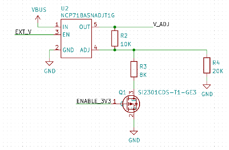
That gets me 1.8 V and 3.3 V out of the LDO. The 5 V case is different — it’s just USB VBUS, a separate rail entirely.
Switching between rails#
Two power domains means a switch between them. And not just any switch: it has to not glitch as I cross over, because the part on the other side is powering the IO of whatever’s connected. Brown out the IO and the module is at best confused, at worst writing garbage to a device.
The textbook solution is a back-to-back MOSFET arrangement with an inverter so one pair is always on and the other always off. TI has a good app note on the topology. It works fine but it’s five MOSFETs plus an inverter, which is more board area than I had.
Instead, I used an FPF1320 — a 2:1 power multiplexer in a 1.4 x 0.96 mm package, with the make-before-break behavior handled internally. One part, one footprint, done.
Where it fell apart#
The plan for the host side was a desktop app that talks to the CY7C65215 over its API and reconfigures it on demand — switch from I2C mode to SPI, set the clock, set the IO voltage, that kind of thing. Infineon ships a configuration tool that does roughly this.
What I didn’t catch until I was deep into it: the runtime API can read and write the device’s internal registers, but it can’t reconfigure the device. Reconfiguring requires their proprietary configuration tool, which generates an encrypted blob and pushes it down.
There was a workaround. Generate a configuration file for every protocol/voltage combination I cared about, encrypt them with Infineon’s tool, then have my app upload the right blob whenever the user changed modes. Ugly but possible.
The real problem was further down. Even if the blob juggling worked, I’d still own a desktop application. Cross-platform. Windows, Linux, macOS. Driver weirdness. Signed binaries. Updates. All for a hobby project whose whole pitch was supposed to be “plug it in and it works.” That’s well outside both my experience and what I want to spend time on.
That should have been the moment I walked.
What I’d do differently#
I should have caught the configuration problem earlier. The CY7C65215’s config flow is built around an OEM setting the part up once during manufacturing — generate a blob with the proprietary tool, encrypt it, flash it. Runtime mode switching wasn’t something the part was designed for. That’s discoverable from the SDK docs if you go looking, but I didn’t go looking until I’d already designed a board around the chip.
The lesson is about how I approach unfamiliar parts on small projects. The instinct on a hobby build is to do one layout, get everything on it, and iterate the whole module. On a chip I know well, that’s fine. On one I’d never used before, with a config flow I hadn’t read carefully, it would have cost almost nothing to wire it up on a breakout first and drive it from a script. The configuration limitation would have surfaced in a week. Instead I found it after laying out a whole board around it.
It wasn’t an expensive mistake on a project this size, but the same shortcut on something larger would have hurt. Next time I’m using a part I don’t know, it goes on a breakout before it goes on a board.
The power topology is solid on its own terms — adjustable LDO with a switched feedback network, plus the FPF1320 for clean handoff between rails. The mistake was committing to an architecture before I’d validated the piece I knew least about.